Vias
Via Styles
Via styles are much the same as pad styles except that only circular or square vias are permitted. The list of via styles is displayed when the Via icon is selected.
New via styles can be created using the New Via Style command on the Library menu. An existing style can be edited by highlighting its name in the object selector and clicking the Edit button.
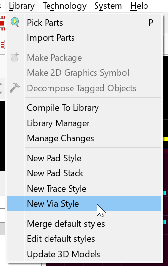
Creating a new via style.
There are two categories of via style:
- Standard (mechanical) via styles are used for through-hole, blind and buried vias that are drilled with a CNC machine. These are the default via styles available in the net class dialogue and the via style selector.
- Micro-via styles have the micro-via flag set, indicating that they are intended for laser-drilled vias on HDI boards. Only circular pad shapes are permitted for micro-via styles; square pads cannot be used. Micro-via styles typically have smaller hole and pad dimensions (for example a 0.1 mm hole with a 0.25 mm pad) reflecting the capabilities of laser drilling. They are kept separate from standard styles in the style selectors and cannot be selected in the net class dialogue.
Micro-vias are also held to a more lenient minimum annular ring than standard vias when the board is checked. The Pre-Production Checklist expects at least 2 thou (0.05 mm) of ring on a micro-via, against 3 thou for a standard via. An oversized micro-via, meaning one with a hole larger than 6 thou (0.15 mm, the IPC-2226 limit for a laser micro-via), is flagged and held to the standard 3 thou ring instead.
In the via style editor the micro-via checkbox is labelled Laser Drilled (HDI), and it is available for circular via styles only. The requirement for the layer stackup to contain at least one micro-via (laser) drill span applies elsewhere: the micro-via controls in the Edit Via dialogue, the DRC room dialogue and the Via Inspector are all disabled on a board with no HDI stackup.
The separation of standard and micro-via styles prevents mismatches between via geometry and drill span type. During routing, micro-via styles are applied through DRC Rooms which override the default via style in specific areas of the board. For a full explanation of how via styles, drill spans and DRC Rooms work together during routing, see Smart Vias & Layer Pairs.
The drill span of a via is decided based on the drill spans specified in the layer stackup for the project. During routing, the smart via algorithm selects the shortest compatible drill span between the source and destination layers. The via style and drill span chosen at placement are defaults; you can always edit a via afterwards to change either.
Via Style Defaults on HDI Boards
On HDI boards, the smart via algorithm excludes micro-via (laser) drill spans from the styles available outside a DRC room. If you route a layer transition that would correspond to a micro-via span, for example Top Copper to Inner 1 on a 1+n+1 board, but the via is not inside a DRC room with a micro-via override, the algorithm will select the shortest legal CNC drill span instead (normally a plated through-hole). This ensures that micro-via styles are only applied in regions where they have been explicitly configured via a DRC room.
Inside a DRC room with a micro-via style override, the algorithm will apply the room's micro-via style whenever the layer transition matches a valid laser drill span. If the transition is incompatible (for example it spans more than one dielectric layer), the room override is not applied and the net class default CNC style is used, with a one-shot warning on the status bar. See Layer Range Compatibility for a detailed worked example.
Tenting or covering of the via is done by setting the guard gap (solder mask opening) to not present. It's a good idea to reflect that in the style name so that you can have multiple styles with the same drill hole and use the tented via style where needed. For example, you may create a V10 style with a 10 thou drill hole and a V10T style representing the tented version. See also Via tenting and filling below.
Once a via has been placed you can perform move / delete / change layer range actions from the right click context menu.
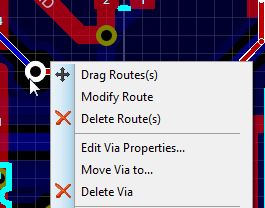
Via editing options on the context menu.
You can also choose to remove annular ring from layers on which there is no connection. See Non-Functional Pads for more information.
See Also:
Stitching & Shielding Zones with Vias
Via stitching ties copper areas on different layers together. It holds the ground planes of a multilayer board at a common low impedance and shortens the return path for signal currents, which in turn reduces radiated emissions. Via shielding places a dense line of vias alongside a sensitive track or around the edge of a copper zone, forming what is often called a via wall or picket fence; its purpose is to isolate a noisy part of the board from a quiet one.
In Proteus both are placed for you. Right click on the edge of a zone or power plane and choose the stitching or shielding option from the context menu, then complete the dialogue form that appears. The vias produced are owned by the zone object, so they are maintained with it, and they are always placed as standard mechanical vias: micro-vias are never used for stitching or shielding. Routes can be shielded with vias in the same way.
Because the vias are owned by the zone rather than placed by hand, the Via Inspector can pick them out with its Shield or Stitch filter, which makes large-scale review and editing straightforward.
Every stitching via adds to the drill count of the board, so a dense fence has a real effect on fabrication cost and time. It is usual to add stitching over broad copper areas late in the design, once routing has settled, since it makes routing harder; a shielding fence around a sensitive track is better planned early so that the space for it is reserved.
See Also:
Example: Stitching Two Zones Together
Example: Shielding a Zone with a Via Fence
Example: Shielding Routes with Vias
Power Planes: Stitching two zones together
Via Tenting and Filling
Via tenting is a simple cover by solder mask and so is achieved by removing the guard gap from the solder resist for that via style.
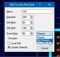
Removing the guard gap from a via style to tent the via.
Proteus supports via filling to the IPC-4761 Type VII standard: the via hole is completely filled (with non-conductive epoxy resin for through-hole vias, or by copper electroplating for micro-vias) and then capped with a thin copper layer that is plated flush with the surrounding pad surface. For micro-vias this is mandatory; for through-hole vias it is an optional design choice controlled by the NCVF tools described below. Blind and buried vias cannot be filled.
Micro-Via Filling
Micro-vias are always marked as filled and capped in Proteus and this cannot be changed. This applies to all micro-vias on the board whether they are via-in-pad or not. In a 1+n+1 HDI construction, each micro-via is laser drilled through the outer buildup layer and must be completely filled and plated over before the outer copper foil is laminated on top. If the via were left open or partially filled, the buildup layer would not present a flat copper surface and the subsequent lamination would fail. Micro-vias are therefore filled by copper electroplating from the target pad upward, and then capped with a thin copper layer that merges flush with the surrounding copper. This is an inherent part of the HDI fabrication sequence rather than an optional step.
Through-Hole Via Filling (NCVF)
For through-hole vias, resin filling and capping (sometimes called NCVF or non-conductive via filling) is an optional process that adds extra steps and cost to board manufacture. It is most commonly used for via-in-pad designs where you don't want solder to wick down the via hole during reflow, typically under fine-pitch BGAs.
There are legitimate reasons not to fill a via-in-pad through-hole via. On lower density boards, or during prototyping, the cost and lead time of the fill, cure, planarise and re-plate cycle may not be justified. If the pad is large enough relative to the hole, or the via sits at the edge of a pad rather than dead centre, solder wicking may be manageable without filling. Some designers also accept a small solder dimple on non-critical pads. These are engineering judgements for the designer to make; Proteus allows filling to be set or unset on a per-via basis to accommodate them.
All filled vias (both micro-vias and resin filled through-hole vias) are output as IPC-4761 Type VII in the Gerber X2 via protection attribute. See Output Systems below for details.
Background Information
IPC-4761 Type VII describes a via that is completely filled and then capped or plated over at the surface, so that the finished pad is flat and solderable and behaves like an ordinary SMT pad. It is the filling that stops solder wicking away down the hole during reflow, which is why it matters most for via-in-pad designs under fine-pitch BGAs.
Filling is a chargeable extra. The fabricator has to fill, cure, planarise and re-plate the board, so expect both additional cost and additional lead time, and expect a minimum finished drill size as well (many fabricators ask for 0.3 mm or more to be confident of a consistent resin fill). State the requirement explicitly in your fabrication notes, for example "All via-in-pad vias to be IPC-4761 Type VII, non-conductive resin filled and capped", rather than relying on the Gerber attribute alone being read.
Resin filling (NCVF) applies to through-hole vias only. Micro-vias are always filled and capped (IPC-4761 Type VII) as part of HDI fabrication and this cannot be changed. Blind and buried vias cannot be filled.
See Also:
Example: Setting Via Filling by Area
Example: Setting Via Filling using Via Inspector
Example: Setting Via Filling on a Single Via
Example: Viewing Filled Vias on the Board
Output Systems
When output as Gerber X2 (recommended) the ViaDrill attribute is set to be type 7 (VII) as specified in the IPC-4761 standard.

The Gerber X2 ViaDrill attribute set to IPC-4761 type VII.
For extra clarity the filled vias will be exported in a separate drill file. If you would rather export them in the same drill file as other through-hole plated vias, uncheck Separate Drill File? in the Via Filling section of the CADCAM output form. Note that VII will still appear as a separate AperFunction:
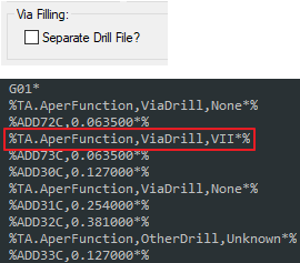
Filled vias carried in the plated drill file with their own AperFunction attribute.
Filled vias are identified in the readme.txt file with a separate toolcode in standard RS274X Gerber. However the technology is newer than the output format so we do not recommend you use RS274X when filled vias are present on the board.
ODB++ output does not carry the filled status of a via. Micro-vias are carried through, flagged as laser drilled, so an HDI stackup survives the export; the fill specification does not, and must be stated in the fabrication notes.
The NCVF option applies to through-hole vias only. Micro-vias are always filled and capped (IPC-4761 Type VII) as part of the HDI fabrication process and this is set automatically by Proteus. Blind and buried vias cannot be filled.
Make sure your layer stack thicknesses are correct. These can be used by the board manufacturer to inform how much epoxy is needed to fill a hole.
Filled vias are also identified in the drill table data object which is placed on the manufacturing report in Project Notes.
Non-Functional Pads
A non-functional pad is just a pad in a printed circuit board that is not connected to a track on the layer it is on. There are three main reasons why you may want to remove these annular rings:
- Space. Makes it easier to subsequently route tracks in tight areas.
- Unwanted or unnecessary capacitance that is significant enough to matter in some designs.
- Easier drilling (the subject of some debate).
Despite the name we almost always mean vias rather than component pin holes and pads when we talk about NFPs, and the tools provided in the software therefore apply to vias only. For component pads you can remove the annular ring on specific layers by creating and using a padstack style.
Terminology
Where a via has the annular ring removed on unused layers we refer it to as a depleted via or sparse via. The non functional pads are the annular rings that are removed.
It is always worth checking with your customer before depleting vias on the board. While IPC-2221 (generic PCB design standard) explicitly allows removal of non-functional pads on inner layers some customers require NFPs to be retained, arguing they add marginal drill support or improve plating uniformity. Others mandate removal to avoid stress risers or capacitance. It is a debated area.
Considerations
Mechanical Considerations
Removing NFPs slightly reduces the amount of copper around drill holes on unused layers. This can reduce copper capture during plating and is sometimes argued to reduce mechanical support for the barrel. For standard commercial PCBs this is usually negligible, but for thick, high-layer-count boards it may be considered.
Electrical Considerations
The capacitance effect of NFPs on unused layers is small but can matter in high-speed or controlled impedance designs. Removing them helps reduce stub-related parasitics, especially in dense via fields under BGAs.
For RF designs, removing NFPs can help keep impedance predictable and reduce via-to-plane parasitic capacitance.
See Also:
Example: Removing Non-Functional Pads
Example: Bulk NFP Removal using Via Inspector
Example: Viewing Depleted Vias
Routing to a Depleted Via
The autorouter will not connect to a depleted via on any layer which has no annular ring. Often this will lead to it being unable to complete and you will end up with missing connections and ratsnest lines.
When routing manually you can connect to a depleted via on a layer which has no annular ring. The annular ring on the tracked layer only will automatically be restored for you when you complete the route.
Non Functional Pads and Design Rules
A non functional pad remains a pad for the purposes of design rules. Where a via has been depleted so that only the drill hole remains the border of the hole is the start of the measurement point for the design rule.
Report Generation
Proteus provides several complementary tools for auditing and documenting the via design on a PCB. Together they allow you to review, verify and communicate the via and drill hole configuration of your board, which is particularly important for HDI designs where micro-vias, filled vias and multiple drill spans must all be clearly specified for the fabricator.
Via Inspector
The Via Inspector is an interactive tool in the PCB editor that provides a filterable, sortable view of every via on the board. It displays the via style, drill span, layer range, hole type, filling status and via-in-pad status for each via and allows bulk editing operations. Use it to:
- Verify that micro-vias are correctly assigned to laser drill spans.
- Confirm filling status across all vias on the board.
- Identify and resolve any unexpected via configurations before generating output.
- Filter by via type (standard, micro-via, filled, via-in-pad) to review specific subsets of the design.
The Via Inspector is a design-time tool: it operates on the live board data and is the primary means of reviewing and editing via properties in bulk.
Drill Table
The drill table is a data widget that can be inserted into any report in Project Notes. It generates a tabular summary of all hole sizes and types on the board, including the count of each, the tool diameter, hole type, plating status, layer range and via classification. The Via/Pad column identifies micro-vias specifically as "Filled Microvia", distinguishing them from standard vias, filled through-hole vias and component pads.
To insert a drill table into a report, use Insert > Project Data from the right click context menu in the Project Notes editor and select Drill Table from the list.
The drill table is most commonly used in the PCB Manufacturing Report template alongside the board stackup and layer stackup views, but it can be added to any Project Notes document. This makes it straightforward to build a comprehensive manufacturing pack that clearly documents the drilling requirements for the board. The table can be regenerated at any time to reflect the current state of the design.
For HDI boards, the drill table provides an at-a-glance summary of the complete drill file set that will be needed for fabrication, covering both CNC-drilled through-holes and laser-drilled micro-vias along with their layer spans and filling requirements. This is especially useful for review before generating CADCAM output.
Microvia Compliance
On HDI boards, a Microvia Compliance data object can be inserted into any Project Notes report alongside the drill table. This widget audits every micro-via on the board against three criteria: drill span validity, filled status and aspect ratio. The aspect ratio warns above 0.75:1, the IPC-2226 recommendation, and fails above 2:1. Each micro-via that fails one or more criteria is listed individually, making it straightforward to locate and correct problems before generating CADCAM output.
For HDI designs, it is good practice to include both a drill table and a Microvia Compliance report in the manufacturing pack. The drill table documents what will be fabricated; the compliance report verifies that the micro-via configuration is correct.
The Pre-Production Checklist runs the same three checks and several more besides, among them a check that each micro-via's style is consistent with the DRC room it sits in, and a check on the annular ring and hole size of every via. Use the checklist for the broader pass/fail summary before output, and insert the Microvia Compliance data object when you want the detailed per-via breakdown in the manufacturing pack.
See Also:
Manufacturing Report: Drill Table